The circuit schematic and PCB layout are different files
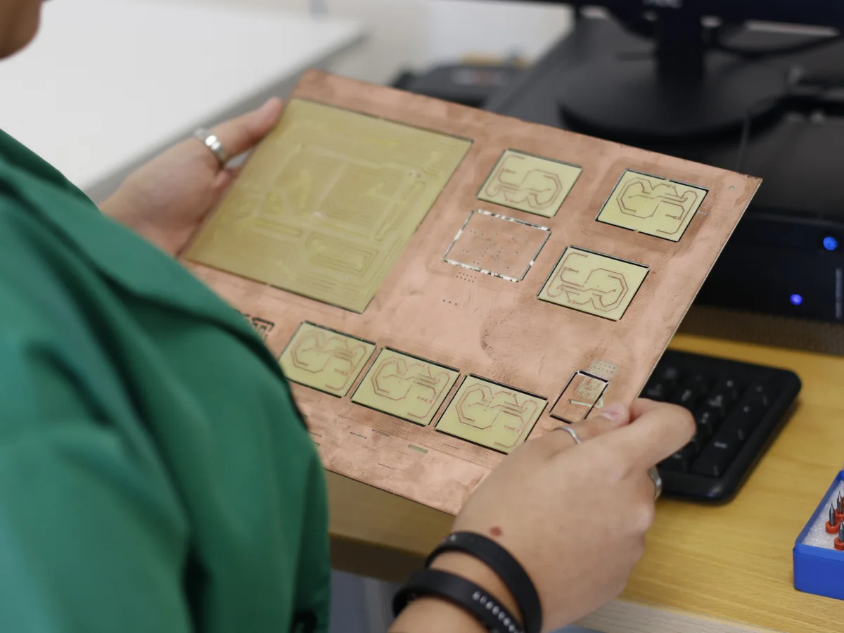
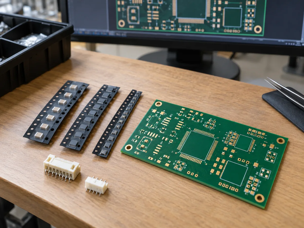
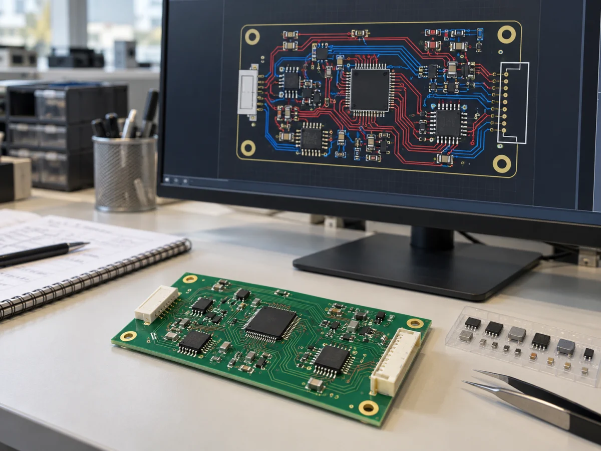
The circuit schematic shows how components are electrically connected. PCB design places those connections on the physical board with defined dimensions and layers. Having a schematic does not mean the layout and all manufacturing outputs are complete. A board photograph or PDF schematic also does not replace an editable design project. Such images help assessment, but the available sources must be evaluated separately before further development.
When commissioning PCB layout, the board outline, mounting holes, connector positions and tall components are coordinated with mechanical design. For a control device with a display, for example, the connector must align with the rear enclosure opening and allow cable insertion. File checks also cover this physical fit. The delivery scope specifies the editable electronics project and, where required, mechanical CAD, library information and approved drawings.